
AI Revolutionizes Semiconductor Manufacturing with Faster Simulations and Smarter Process Control
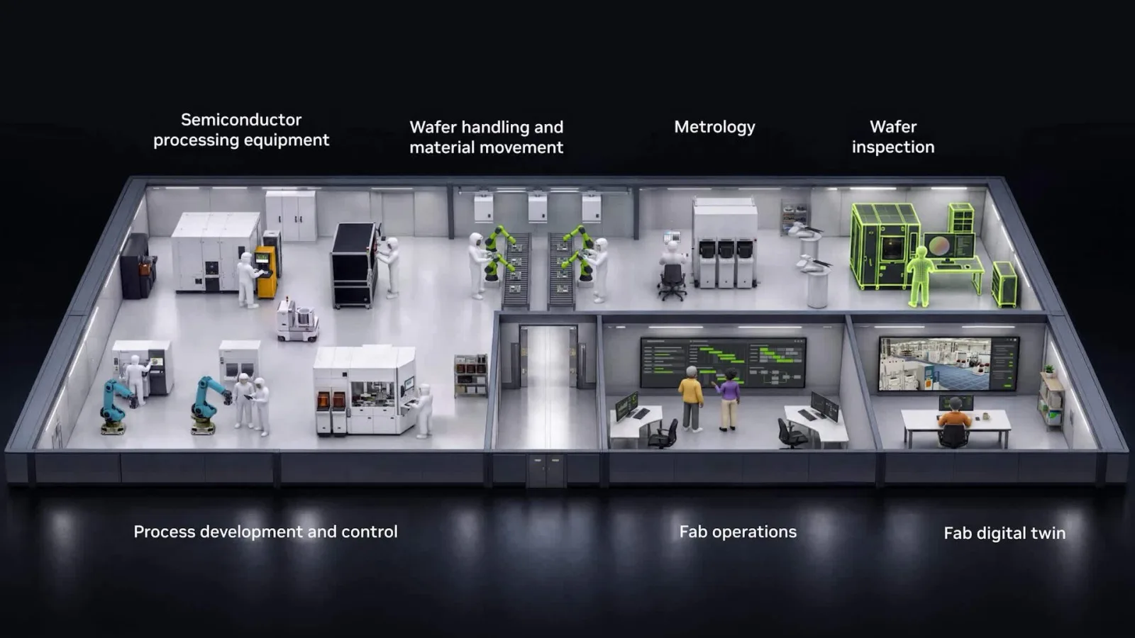
Image: NVIDIA · Source
AI technologies are transforming semiconductor fabs by accelerating simulations, predicting process behaviors, automating engineering workflows, and enabling digital twins, thereby helping engineers optimize complex chip manufacturing processes more quickly and accurately.
The ever-increasing demand for advanced semiconductor chips requires more complex manufacturing processes, where even minor errors can have significant impacts on yields and product quality. Engineers face the challenging task of understanding how process changes and material interactions affect overall outcomes, often relying on time-consuming physical experiments and simulations.
Artificial intelligence (AI) is now playing a pivotal role in reshaping semiconductor fabrication. Leveraging accelerated computing, AI dramatically shortens simulation times. This not only speeds individual calculations but also expands the range of alternatives that engineers can evaluate before committing to physical trials. For instance, multiphysics simulations involving heat transfer, electrical effects, and mechanical stresses—critical to optimizing equipment and processes—are running up to 10 times faster using NVIDIA's cuDSS library, as noted by COMSOL.
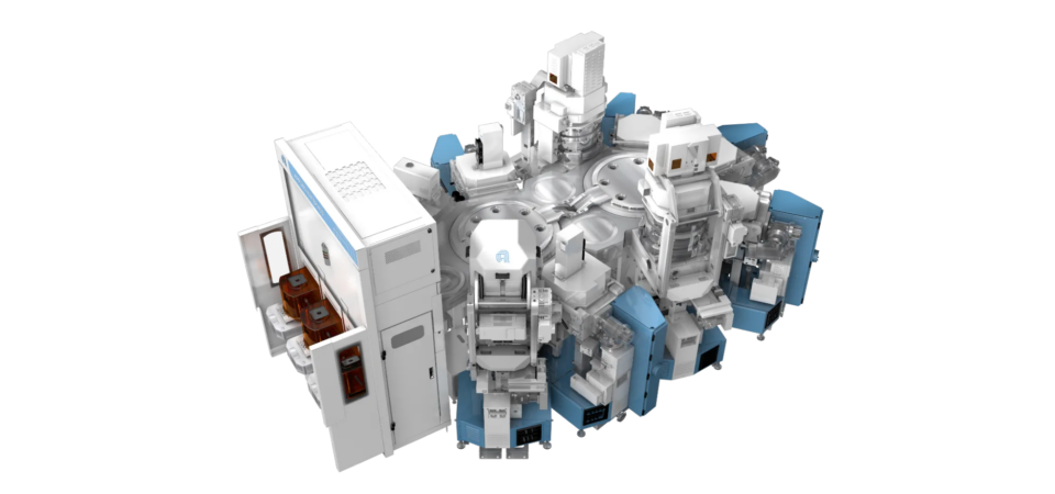
Collaborations between NVIDIA and companies like Applied Materials further enhance atomic-scale materials discovery and process development. Applied's Ginestra and ACE+ multiphysics platforms, integrated with NVIDIA technologies, achieve speedups up to 10x and 35x respectively compared to CPU-based methods. Meanwhile, Siemens integrates NVIDIA's cuLitho into its Calibre lithography software, accelerating computational lithography tasks by up to 17 times, which expands the scope of pre-production verification engineers can perform on circuit patterns.
Beyond accelerating simulations, AI systems trained on physics principles can predict complex process behaviors without running full simulations every time. Lam Research demonstrates this with plasma behavior modeling—a computationally intensive task—predicting outcomes within milliseconds rather than days using NVIDIA’s PhysicsNeMo framework.
AI also streamlines the workflows between engineering decisions. Complex choices like selecting appropriate AI models for specific tasks, which previously took hours manually, are now automated and reduced to minutes with NVIDIA NeMo Switchyard AI agents, as Advantest employs.
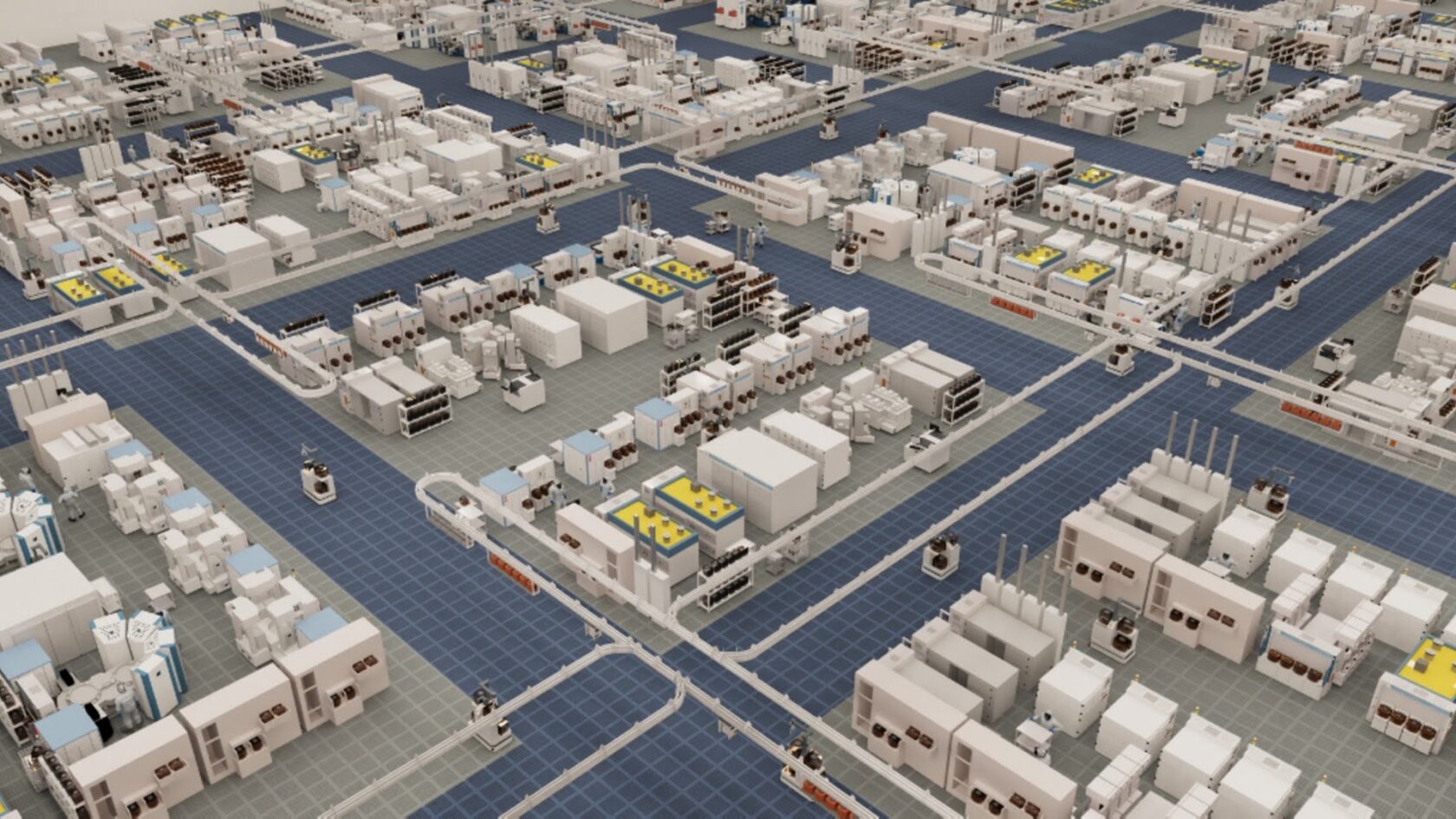
Furthermore, digital twins—virtual replicas of fabs—are enabling teams to test equipment configurations, material flows, and process changes without costly physical trials. Applied Materials utilizes NVIDIA Omniverse to create highly accurate digital twin models, allowing comprehensive factory-wide simulations to identify bottlenecks and optimize layouts.
The integration of these AI-driven capabilities into an "AI-defined fab" represents the future of semiconductor manufacturing. It enables a connected loop where production data continuously refines predictive models, which in turn inform engineering decisions earlier, enhancing yield, quality, and throughput. Overall, AI empowers engineers to move faster and make better-informed decisions throughout the semiconductor manufacturing lifecycle, addressing the challenges posed by ever more complex fabrication processes.
Sources and original reporting
Read the original source ↗
Comments (0)
No comments yet. Start the discussion.
Write a comment
Comments are published after moderation. Your name and comment will be visible publicly. Account